- 您现在的位置:买卖IC网 > Sheet目录3753 > ATMEGA169P-16MCHR (Atmel)MCU AVR 16KB FLASH 16MHZ 64-VQFN
PIC16F946
DS41265A-page 244
Preliminary
2005 Microchip Technology Inc.
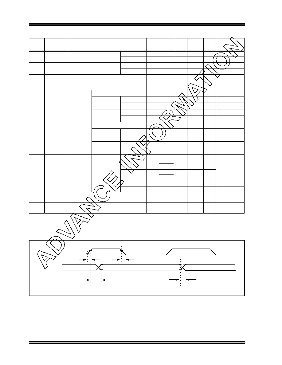
TABLE 19-5:
TIMER0 AND TIMER1 EXTERNAL CLOCK REQUIREMENTS
FIGURE 19-8:
USART SYNCHRONOUS TRANSMISSION (MASTER/SLAVE) TIMING
Param
No.
Sym
Characteristic
Min
Typ
Max
Units
Conditions
40*
TT0H
T0CKI High Pulse Width
No Prescaler
0.5 TCY + 20
—
ns
With Prescaler
10
—
ns
41*
TT0L
T0CKI Low Pulse Width
No Prescaler
0.5 TCY + 20
—
ns
With Prescaler
10
—
ns
42*
TT0P
T0CKI Period
Greater of:
20 or TCY + 40
N
—
ns
N = prescale
value (2, 4, ...,
256)
45*
TT1H
T1CKI High
Time
Synchronous, No Prescaler
0.5 TCY + 20
—
ns
Synchronous,
with Prescaler
3.0-5.5V
15
—
ns
2.0-5.5V
25
—
ns
Asynchronous
3.0-5.5V
30
—
ns
2.0-5.5V
50
—
ns
46*
TT1L
T1CKI Low
Time
Synchronous, No Prescaler
0.5 TCY + 20
—
ns
Synchronous,
with Prescaler
3.0-5.5V
15
—
ns
2.0-5.5V
25
—
ns
Asynchronous
3.0-5.5V
30
—
ns
2.0-5.5V
50
—
ns
47*
TT1P
T1CKI Input
Period
Synchronous
3.0-5.5V
GREATER OF:
30 OR TCY + 40
N
—
ns
N = prescale
value (1, 2, 4, 8)
2.0-5.5V
50 OR TCY + 40
N
——
ns
Asynchronous
3.0-5.5V
60
—
ns
2.0-5.5V
100
—
ns
FT1
Timer1 oscillator input frequency range
(oscillator enabled by setting bit T1OSCEN)
DC
—
37*
kHz
48
TCKEZTMR1 Delay from external clock edge to timer
increment
2 TOSC*—
7 TOSC*—
*
These parameters are characterized but not tested.
Data in ‘Typ’ column is at 5V, 25°C unless otherwise stated. These parameters are for design guidance only and are not
tested.
Note:
Refer to Figure 19-2 for load conditions.
121
120
122
RC6/TX/CK
RC7/RX/DT/
SCK/SCL/SEG9
SDI/SDA/SEG8
发布紧急采购,3分钟左右您将得到回复。
相关PDF资料
2-1546217-0
TERM BLK RCPT 20POS SIDE 5.08MM
1-1546217-9
TERM BLK RCPT 19POS SIDE 5.08MM
1-1546217-8
TERM BLK RCPT 18POS SIDE 5.08MM
1-1546217-7
TERM BLK RCPT 17POS SIDE 5.08MM
1-1546217-6
TERM BLK RCPT 16POS SIDE 5.08MM
1-1546217-5
TERM BLK RCPT 15POS SIDE 5.08MM
1-1546217-4
TERM BLK RCPT 14POS SIDE 5.08MM
1-1546217-3
TERM BLK RCPT 13POS SIDE 5.08MM
相关代理商/技术参数
ATMEGA169P-16MCU
功能描述:8位微控制器 -MCU AVR 16KB, 512B EE 16MHz 1KB SRAM, 5V
RoHS:否 制造商:Silicon Labs 核心:8051 处理器系列:C8051F39x 数据总线宽度:8 bit 最大时钟频率:50 MHz 程序存储器大小:16 KB 数据 RAM 大小:1 KB 片上 ADC:Yes 工作电源电压:1.8 V to 3.6 V 工作温度范围:- 40 C to + 105 C 封装 / 箱体:QFN-20 安装风格:SMD/SMT
ATMEGA169P-16MU
功能描述:8位微控制器 -MCU AVR 16K FLASH 512B EE 1K SRAM LCD ADC RoHS:否 制造商:Silicon Labs 核心:8051 处理器系列:C8051F39x 数据总线宽度:8 bit 最大时钟频率:50 MHz 程序存储器大小:16 KB 数据 RAM 大小:1 KB 片上 ADC:Yes 工作电源电压:1.8 V to 3.6 V 工作温度范围:- 40 C to + 105 C 封装 / 箱体:QFN-20 安装风格:SMD/SMT
ATMEGA169P-16MU SL383
制造商:Atmel Corporation 功能描述:MCU 8BIT ATMEGA RISC 16KB FLASH 3.3V/5V 64PIN MLF - Tape and Reel
ATMEGA169P-16MUR
功能描述:8位微控制器 -MCU AVR LCD 16KB FLSH EE 512B 1KB SRAM-16MHZ RoHS:否 制造商:Silicon Labs 核心:8051 处理器系列:C8051F39x 数据总线宽度:8 bit 最大时钟频率:50 MHz 程序存储器大小:16 KB 数据 RAM 大小:1 KB 片上 ADC:Yes 工作电源电压:1.8 V to 3.6 V 工作温度范围:- 40 C to + 105 C 封装 / 箱体:QFN-20 安装风格:SMD/SMT
ATMEGA169P-8AU
制造商:ATMEL 制造商全称:ATMEL Corporation 功能描述:Microcontroller with 16K Bytes In-System Programmable Flash
ATMEGA169P-8MU
制造商:ATMEL 制造商全称:ATMEL Corporation 功能描述:Microcontroller with 16K Bytes In-System Programmable Flash
ATMEGA169PA
制造商:ATMEL 制造商全称:ATMEL Corporation 功能描述:8-bit Microcontroller with 16K Bytes In-System Programmable Flash
ATMEGA169PA_1
制造商:ATMEL 制造商全称:ATMEL Corporation 功能描述:High Endurance Non-volatile Memory segments